
The Core of a GK110 Based Video Card.
The Graphics Processor Unit.
There are very few area’s of desktop computing that have seen the kind of explosive development that Graphics cards have undergone. The most modern and highest end video cards are in effect self contained computer systems that contain phenomenal computational power especially when compared to modern CPU’s. But these devices have extremely simple beginnings with the very earliest devices being little more than a small chip that allowed a computer to display white text on a black or green screen. The Windows command prompt is in part a throw-back to those early days and modern Graphical User Interfaces have only become possible due to the explosive advances in the field of GPU technology.
Understanding the Basics.
Modern Video cards comprise of a circuit board that may be designed by the supplier of the card or may be manufactured to the specification of the manufacturer of the GPU. Boards that are manufactured to the specification of the GPU provider are referred to as reference boards or reference cards. The card will have an edge connector which fits into a specific slot on the computer, modern cards are designed to be installed into one of the PCIe 3.0 slots on modern computer motherboards.

An Asus Motherboard. The PCIe3 Slots are highlighted in green
The PCIe 3.0 Slot highlighted in green in the above image is the longest on the motherboard and that should tell you something regarding the processing capacity of a modern Video Card. These slots carry the largest number of ‘data lanes’ these are pathways that carry data to and from the CPU and the main memory of the computer. Generally the more that are available the less inhibited the cards performance will be. All modern Video cards carry their own RAM, but the RAM used by Video Cards is quite different from the standard memory used in a modern computer. Most PC’s use DDR3 RAM, it is reasonably cheap and given the level of processing capability in today’s CPU’s it is more than adequate for the task. However Video Cards use GDDR5 RAM. This RAM is difficult to produce, extremely fast, and relatively expensive though it is well suited to the higher level processing throughput of a modern Video Card.
The Need for Speed
Until fairly recently the Intel 3960X CPU was the fastest commercial desktop class processor that Intel produced. It had 6 Processor cores, 15Mb of onboard cache and utilisied an Intel technology known as Hyperthreading. It has 2.3 Billion Transistors and a total compute performance of around 316 Gigaflops. A Gigaflop being a word that describes the number of computational operations per second (ops) that a device can process in this case the number can be expressed as 10 to the power 9, or if you prefer a 1 followed by nine 0’s meaning that this chip can calculate 316 Billion (316,000,000,000) mathematical operations a second.
Nvidia’s GeForce Titan GPU has 6GB of GDDR5 RAM, 2,688 Cores and consists of 7.1 Billion Transistors and has a total compute performance of 4,500 Gigaflops or 4.5 Terraflops meaning this chip can calculate 4,500,000,000,000 mathematical operations per second. Modern GPU’s are more than 11-12 times more powerful than the fastest desktop Processors. But it wasn’t always so…
ISA
The Industry Standard Architecture was a standard interface and bus technology introduced in the early 1980’s by IBM for the PC to support Intel 8088 processors. It originated as an 8 bit external bus that was extended to 16 Bits for the Intel 80286 CPU. It was conceived and designed as a method to allow PC owners to add extra devices to their computer’s to extend the functionality of their computers. But it was (by modern standards) inconceivably limited. For example ISA permitted only the first 16MB of main system RAM to be accessed by any additional devices. Additionally the 8 Bit bus ran at a meagre 4.77Mhz while the extended 16Bit bus ran at between 6 and 8Mhz.
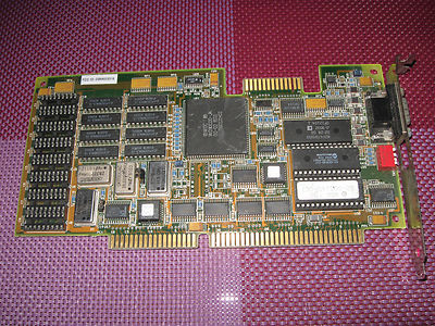
Western Digital ‘Paradise’ Video Card
This is a Western Digital Paradise Video card, given the number of Memory modules mounted on the board, I’d estimate that this card has a huge 1Mb of RAM. it was capable of displaying a maximum of 256 colours with a refresh rate of 43hz which is too low to function a modern LCD panel. Device’s like these formed the basis of the modern graphics card.
But it was the drive for increased performance, primarily led by incoming graphical user interfaces for business use, that resulted in the next major development in Graphics card technology. The VESA Local Bus.
Video Electronics Standards Association Bus
In the late 80’s the ISA bus was becoming the critical straining or bottleneck point in modern PC’s. Simply put ISA could not deliver the performance required by the ever more sophisticated graphically driven software that was becoming increasingly prominent. Something had to be done, and it was. This led to the development of a higher performance bus combined with a specific extended slot dedicated to video hardware. The VESA Bus, though it’s adoption was not uncomplicated.
At the time the VESA bus appeared IBM developed its own alternative, known as Micro Channel Architecture. The IBM technology was more than feasible, but it was utterly proprietary and came with large license fee demands for manufacturers. At the time it was technically illegal to reverse engineer the connector standard to construct MCA compliant cards and this choked the development of high speed video processors for the standard. The other competing standard was EISA. Extended ISA basically extended the slot length and therefore theoretically, the number of signal lanes to the slot, but it couldn’t deliver sufficient performance resulting in a clear market path for VESA to succeed. However as a solution VESA was extremely limited.
To much credit and not enough VESA???
VESA was designed solely as a stop-gap solution to the problem of constrained data bandwidth between the video adapter and the computer. Simply put the software becoming available at the time was placing to high a demand on the hardware that supported existing video cards, irrespective of the sophistication of the card. The underlying hardware simply couldn’t meet the demand. Not unlike going out and buying a million dollar home when you only earn $10,000 a year, eventually the repayment’s will catch up with you. Additionally the major principle requirement for VESA’s establishment was that it should not be cost prohibitive to implement. VESA Was introduced alongside the stunning (at the time) Intel 486 processor and tied a VESA Local Bus (VLB) card directly to the CPU with very little by way of interfacing technologies or logic. This simplicity not only led to adoption, but the next hurdle.
The Intel 486 CPU.
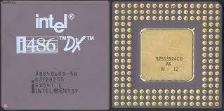
The Intel 486 CPU
Because the VESA Local Bus was so heavily dependent upon the Intel 486 processor’s memory design this resulted in it being eventually dropped in the Pentium or 586 generation CPU’s. Additionally machines that shipped with VLB slots usually had at most 2 VESA slots available, severely limiting the expansion potential of the system even though they still carried 3 or 4 other slower ISA slots too.
Power
But the most limiting factor of all was simply power. Due to the direct nature of the VLB and its direct interface pathways to the CPU and Memory, the electrical load of the card was massively constrained limiting the end results of what was practically possible with the devices. The VESA devices also had excessively long slots and therefor excessively long edge connectors and this made installation of the cards a delicate and often tricky operation.
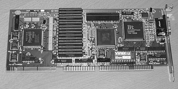
VESA Local Bus Video Card
These cards were over 30 cm. long and featured edge connectors through the entire length of the device. Clearly a new standard would be required for a new generation of hardware and when the 486 entered the pages of Technological history so did VESA.
The Pentium Generation.
The Pentium Processor
In order to meet the demands of modern applications and increase the performance of the computer system as a whole Intel embarked on one of the most radical overhauls of it’s technology to date. Even now there are hallmarks of the Pentium CPU core to be found in modern PC’s. Welcome to the modern age of the Personal Computer.
Notable for its well publicised calculation flaw when introduced, the Pentium also saw the introduction of the PCI Local Bus.
Peripheral Component Interconnect
PCI originally started to appear in Server’s due to the enhanced performance and power envelope introduced by the new standard. These features bade well for high performance applications. but it wasn’t really until 1994 that adoption in desktop PC’s became mainstream. The PCI Bus was self configuring with separate address and memory spaces to support the x86 family of processors. PCI also allowed devices installed in the card slots to carry their own ROM (a chip containing some basic software) that could assist the system at startup to bring the hardware to a functional level. PCI Also started to see the introduction of specific 3D Graphics hardware such as the 3DFX card, one of the first 3D Graphics accelerator boards.
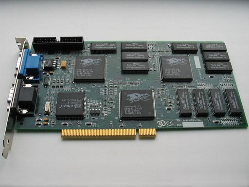
3DFX Voodoo PCI Video card
Originally however the PCI Bus was shared which meant it was possible for a single device to choke the system. With the increasing sophistication of hardware the chances of this occurring became increasingly likely. When developing the next platform standard Intel noted the accelerated development cycles that Video hardware was undergoing. This lead to the eventual development of the AGP (Accelerated Graphics Port) Bus which was a single high speed slot dedicated to Graphics cards. As the graphical competency of computer’s was expected to grow, so did the performance requirements placed on the hardware that supported the devices. The choke point issues with PCI were overcome by assigning this single specific AGP bus for the task.
AGP featured direct access to the CPU rather than having to share access with other devices on the PCI Bus. In addition to this, the direct connection allowed the video card to communicate with the CPU at a much higher rate /clock speed than had traditionally been possible. It was also possible for these devices to directly access the system RAM to load data directly using a concept known as the Graphics Address Remapping Table. This allowed the video card to reclaim or re-apportion segments of system RAM to service its needs. AGP became the defacto graphics standard from around 2000 to 2004 when it started to be phased out in preference for PCI Express (PCIe).

AGP, PCI, PCIe Slots together
The need for speed… (Or back where we started)
In 2004 the PCI Express (PCIe) bus finally started to become to defacto standard for virtually every device on a modern computer. It shared the AGP Bus approach in that it used separate data buses for devices instead of the limited single shared bus with the original PCI standard. With the principal differences being implied simply by the length of the slot.
PCIe remains with us today and the slots now come in different ‘lengths’ measured as PCIe 3.0 x1, x2 or x3. The x1 slots are the smallest and are generally reserved for low bandwidth cards such as Sound and Network hardware. Most commonly modern GPU’s are hosted in the x3 slot’s to service their increased data requirements. Since these slots have more direct connections to both the CPU and the system RAM ostensibly increasing their throughput significantly.
However, most modern video cards have even outgrown this and are now almost complete systems on a board, with their own Processor, RAM and Bus to service their own internal needs. They even feature their own power connectors because their requirements outstrip the meagre power supplied by the system board. The only time the cards really need to use the bus is if it needs to access the CPU or pull data out of the PC system’s RAM.
